
 採用情報
採用情報 お問い合わせ


サービスの特徴
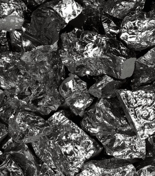
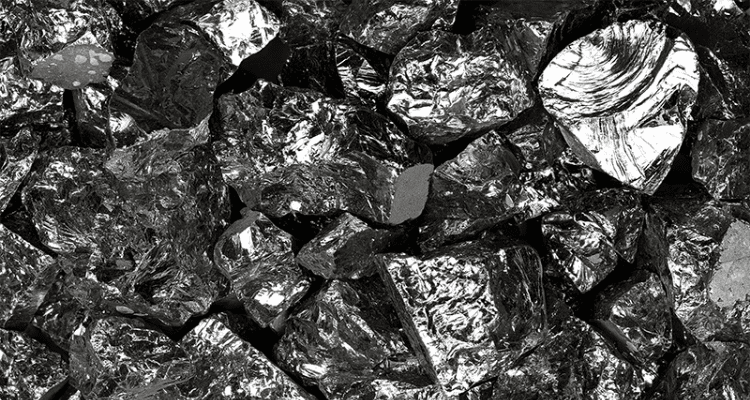
貴重な素材である「シリコン」の
リサイクルで
地球規模のエコに貢献しています
永輝商事では、シリコン精製メーカーから不要となったシリコンを買い取り、太陽光発電設備の原材料としてリサイクルする事業を行っています。半導体に欠かせない素材であるシリコン(ケイ素)は自然界に多数存在する元素ですが、半導体に使用する際には「99.999999999%」(イレブン・ナイン)という超高純度の精製が必要となります。対して太陽光発電設備の原材料として求められる純度は「99.9999%」(シックス・ナイン)と大きな違いがあり、シリコン精製メーカーが半導体メーカーへ提供できなくなってしまった純度の原材料でも、再び活用できるのです。
2020年以降は新型コロナウイルスの影響もあり世界的に半導体の供給が不足しています。同時に原材料であるシリコンも品薄の状態が続き、太陽光発電設備の生産体制にも大きな影響をおよぼしています。シリコンをリサイクルできることは社会的にも大きな意義を持ち、廃棄物を減らすことで地球規模のエコにもつながっています。
当社の強み
国内だけでなく
海外へも広範なネットワークを築き、
リサイクルシリコンの供給を進めています
従来、シリコン精製メーカーでは、半導体生産に必要な純度を満たさないシリコンが不要物として廃棄されていました。私たちはこれらを有価物として買い取ることで、廃棄物の削減とともにシリコン精製メーカーのコスト削減にも寄与しています。買い取ったシリコンは厳密な検品と選別を経て、自社グループ内の太陽光発電設備製造に活用しているほか、他の太陽光パネルメーカーやインゴット(金属シリコン)メーカーなどへの販売も行っています。リサイクルされたシリコンは貴重な素材として、幅広い用途に使われるようになりました。
私たちが広範囲にわたってシリコンリサイクルの流通に携われるのは、日本国内はもとより、海外にも綿密なネットワークを有しているからです。永輝商事で働くメンバーは、国内拠点においても約半数が海外出身。中国やマレーシア、インド、ベトナムなど、多様な国籍の人材が連携して、世界各地への橋渡し役を担っています。
このような
お悩みありませんか?
永輝商事では
半導体・シリコンの高価買取実施中!
まずはお気軽にご相談ください。


リサイクル可能な半導体・シリコン
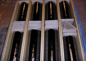
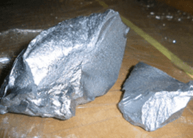
単結晶 インゴット
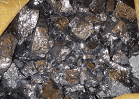
ポリシリコン
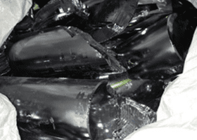
ポットスクラップ
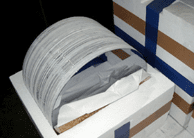
単結晶トップ&テール
丸ウェーハ
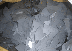
割れウェーハ
